Fujifilm has plans to invest a hefty sum of 20 billion yen in its semiconductor materials business with an aim to further strengthen its facilities for the development, production and quality evaluation of advanced semiconductor materials in Shizuoka and Oita, Japan.
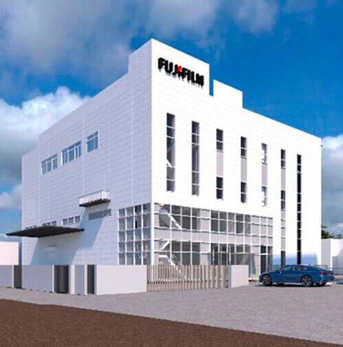
Image of the new building at the Oita site in Japan.
(Source: Fujifilm)
Tokyo/Japan – Fujifilm Corporation has recently made an investment of 20 billion yen in its semiconductor materials business to further strengthen its facilities for the development, production and quality evaluation of advanced semiconductor materials in Shizuoka and Oita, Japan. The total amount of capital investment is approximately 20 billion yen.
Driven by high-speed, high-capacity communications through 5G/6G, the expansion of autonomous driving, and the spread of AI and the metaverse, demand for semiconductors is expected to increase and their performance is projected to advance as well. Consequently, ensuring a stable supply of higher quality and higher performance semiconductor materials for the semiconductor manufacturing process has become increasingly critical.
Fujifilm offers semiconductor materials used in wafer processing to post processing in semiconductor manufacturing including photoresists, photolithography-related materials, CMP slurries, post-CMP cleaners, thin-film chemicals and polyimides, as well as Wave Control Mosaic which includes color filter materials for image sensors.
In addition to its extensive product lineup covering almost the entire range of semiconductor manufacturing processes, from leading-edge to legacy semiconductors, Fujifilm is committed to solving customers' issues by providing one-stop solutions that leverage its global supply structure and advanced R&D capabilities. At the same time, the company is making aggressive capital investments in production facilities globally, and is expanding production capacity of semiconductor materials.
Fujifilm Electronic Materials Co., the core company that leads Fujifilm’s semiconductor materials business, will strengthen and expand its sites in Shizuoka and Oita to enhance the development, production, and quality assurance of advanced semiconductor materials.
Stay up to Date
Do you want the latest news, specialist articles and information on new products? Then you can register for our free newsletter:
At the Shizuoka site, Fujifilm Electronic Materials invests approximately 13 billion yen to construct a new building to strengthen the development, production and quality evaluation functions for advanced photoresists, including photoresists for extreme ultraviolet lithography (EUV), and Wave Control Mosaic. The new building will be equipped with the clean room and state-of-the-art inspection equipment. With the new facility, the company will further speed up development, expand production capacity, and enhance its quality evaluation systems.
At the Oita site, Fujifilm Electronic Materials invests approximately 7 billion yen to construct a new building, acquiring land adjacent to the existing site. It will introduce additional production equipment and inspection devices for post-CMP cleaners, which are key materials in the semiconductor manufacturing process. This will expand the production capacity at the Oita site by approximately 40 %. Post-CMP cleaners are used in the process of uniformly flattening the surface of semiconductors. Post-CMP cleaners are used after polishing with CMP slurry to remove particles, minute metal fragments and organic residues while protecting the metal surface, and the market is expected to grow at an annual rate of 9 %.
Fujifilm will aim to further expand its business as the equipment enhancement enables more stable and rapid supply of post-CMP cleaners. In addition, by making the most of its strength in being able to propose post-CMP cleaners in combination with CMP slurry to customers, it will enhance its contribution to solving the customers’ issues and further improvements in semiconductor performance.
The new building at the Shizuoka site is scheduled to begin operations in the fall of 2025, and the new building at the Oita site is scheduled to begin operations in the spring of 2026.
Fujifilm will continue to contribute to the further development of the semiconductor industry by accelerating the development and the stable supply of semiconductor materials that cover a wide range of products, from leading-edge to legacy semiconductors.
Date: 08.12.2025
Naturally, we always handle your personal data responsibly. Any personal data we receive from you is processed in accordance with applicable data protection legislation. For detailed information please see our privacy policy.
Consent to the use of data for promotional purposes
I hereby consent to Vogel Communications Group GmbH & Co. KG, Max-Planck-Str. 7-9, 97082 Würzburg including any affiliated companies according to §§ 15 et seq. AktG (hereafter: Vogel Communications Group) using my e-mail address to send editorial newsletters. A list of all affiliated companies can be found here
Newsletter content may include all products and services of any companies mentioned above, including for example specialist journals and books, events and fairs as well as event-related products and services, print and digital media offers and services such as additional (editorial) newsletters, raffles, lead campaigns, market research both online and offline, specialist webportals and e-learning offers. In case my personal telephone number has also been collected, it may be used for offers of aforementioned products, for services of the companies mentioned above, and market research purposes.
Additionally, my consent also includes the processing of my email address and telephone number for data matching for marketing purposes with select advertising partners such as LinkedIn, Google, and Meta. For this, Vogel Communications Group may transmit said data in hashed form to the advertising partners who then use said data to determine whether I am also a member of the mentioned advertising partner portals. Vogel Communications Group uses this feature for the purposes of re-targeting (up-selling, cross-selling, and customer loyalty), generating so-called look-alike audiences for acquisition of new customers, and as basis for exclusion for on-going advertising campaigns. Further information can be found in section “data matching for marketing purposes”.
In case I access protected data on Internet portals of Vogel Communications Group including any affiliated companies according to §§ 15 et seq. AktG, I need to provide further data in order to register for the access to such content. In return for this free access to editorial content, my data may be used in accordance with this consent for the purposes stated here. This does not apply to data matching for marketing purposes.
Right of revocation
I understand that I can revoke my consent at will. My revocation does not change the lawfulness of data processing that was conducted based on my consent leading up to my revocation. One option to declare my revocation is to use the contact form found at https://contact.vogel.de. In case I no longer wish to receive certain newsletters, I have subscribed to, I can also click on the unsubscribe link included at the end of a newsletter. Further information regarding my right of revocation and the implementation of it as well as the consequences of my revocation can be found in the data protection declaration, section editorial newsletter.




:quality(80)/p7i.vogel.de/wcms/20/9b/209b81269c3b7255e1f49c5771cfc303/0133747923v2.jpeg "Under the theme \"Step into Cognitive Manufacturing\", Ima will present its vision of a new generation of manufacturing, where Artificial Intelligence, advanced Robotics, Digital Vision Systems and Human Expertise work together to create smarter, more connected and adaptive production environments. (Source: Ima)")
:quality(80)/p7i.vogel.de/wcms/e5/87/e587bb7a91212bcc1ae875ef1bbb6edf/0133471290v2.jpeg "Physical AI marks a shift from machines that follow fixed instructions to embodied systems that perceive, reason, and act autonomously. (Source: Pixabay)")
:quality(80)/p7i.vogel.de/wcms/8b/a5/8ba5d7e346543b30d3066de20e059c59/0133394741v2.jpeg "Currently under construction in Delfzijl, the new SAF facility will support the Netherlands’ efforts to meet the EU’s sustainable aviation fuel mandate. (Source: Emerson )")
:quality(80)/p7i.vogel.de/wcms/6f/90/6f90a6bb14694e7597ec1234110da041/0133293480v2.jpeg "Under the MOU, Aramco will provide domain knowledge, data, and infrastructure to evaluate Sony’s technologies in real-world industrial settings. (Source: Aramco )")
:quality(80)/p7i.vogel.de/wcms/5e/0f/5e0f355d4e90ad6e1af1c997b8789b7d/0133748771v2.jpeg "Elkem Rana’s second furnace will operate as normal during the period. (Source: Elkem )")
:quality(80)/p7i.vogel.de/wcms/c8/30/c830ea0047f500d4c8e9b1a39744d05c/0133653487v2.jpeg "Technip Energies has been awarded contracts by Petkim, a subsidiary of Socar, in connection with the development of a proposed integrated petrochemical complex in Aliağa, Türkiye. (Source: Pixabay)")
:quality(80)/p7i.vogel.de/wcms/56/9d/569db69474e60a709992a9ae5a94ff78/0133613642v2.jpeg "Avantium has successfully produced the first batch of FDCA at its FDCA flagship plant in Delfzijl, the world's first commercial-scale plant for the production of FDCA. (Source: Unsplash)")
:quality(80)/p7i.vogel.de/wcms/2d/ff/2dff64eb5e03d787ed12706e1f344da7/0133613610v2.jpeg "The scope of work includes the development of the engineering design package, the definition of the key technical requirements and the cost estimation for the project. (Source: Pixabay)")
:quality(80)/p7i.vogel.de/wcms/c3/40/c340a3cd06990549f48cf68ae3c5ffff/0133748269v2.jpeg "Bayer has plans to invest 2.2 billion dollars in a new pharmaceutical manufacturing site in New Albany, Ohio, U.S. (Source: Bayer )")
:quality(80)/p7i.vogel.de/wcms/87/4a/874ac98c92c3cab99c0cb57a812caa80/0133555719v2.jpeg "The VPHP Bioindicator is based on spores of Geobacillus stearothermophilus ATCC 12980 and uses packaging permeable to VPHP. (Source: Ima)")
:quality(80)/p7i.vogel.de/wcms/53/a4/53a447ccf82236286a9c98307cd7fa81/0133438889v2.jpeg "The OEB5-contained capsule filling machine is integrated with an isolator and processes solid and liquid oral formulations. (Source: Marchesini)")
:quality(80)/p7i.vogel.de/wcms/02/2c/022cab680492112fbf0ef42892dddd63/0133748297v2.jpeg "In addition to production of green hydrogen, the H2future-Follow-Up project is now increasingly focusing on its treatment and provision for industrial applications. (Source: Verbund)")
:quality(80)/p7i.vogel.de/wcms/54/b9/54b9798cdc66e4aa54009dcd5fd2a682/0133616385v2.jpeg "Hydrogen production plant using water electrolysis powered by renewable energy. (Source: Hyundai E&C/AI-generated image)")
:quality(80)/p7i.vogel.de/wcms/c5/03/c5039bd2b47b209d1112fcc5227d04fc/0133537580v2.jpeg "The facility is expected to strengthen Manatee County’s position as a strategic energy and logistics hub. (Source: Unsplash)")
:quality(80)/p7i.vogel.de/wcms/67/ef/67efeaefe508d0fba36d39f65e0ff406/0133485604v2.jpeg "Once captured, CO₂ is liquefied, delivered by truck to a dedicated CO₂ terminal at Port Esbjerg, shipped aboard Carbon Destroyer 1 - the EU's first purpose-built CO₂ carrier - and injected into the Nini West reservoir. (Source: Ineos Energy )")
:quality(80)/p7i.vogel.de/wcms/7f/1b/7f1b02563e4803ee7f3764ffd1720d8c/0132842468v3.jpeg "The new EZJetFlo™ in-line mixing system solves the production bottleneck using highly efficient Venturi powder induction. (Source: ILC DOver)")
:quality(80)/p7i.vogel.de/wcms/02/fb/02fbe7296b87b2c110ad17e983d7d87a/0132963781v2.jpeg "MAAG’s Extrex6 EC gear pump is specifically designed for the continuous conveying of rigid PVC (polyvinyl chloride). (Bild: Maag)")
:quality(80)/p7i.vogel.de/wcms/69/8c/698c17b920244559c08f28261636fee5/0132816720v2.jpeg "Xylem has entered into an agreement to acquire the Cornell Pump and Roper Pump businesses from Indicor for 1.46 billion dollars. (Source: Pixabay)")
:quality(80)/p7i.vogel.de/wcms/89/47/8947595eafaa6ad27c8552a5f9ad48e1/0129967379v1.jpeg "Biogas and biomethane currently provide approximately 5.5 GW of stable electrical capacity and could be expanded to up to 20 GW without requiring additional land – an enormous potential. (Source: license free via Pixabay)")
:quality(80)/p7i.vogel.de/wcms/fe/5d/fe5d9bb106dfb20c1d69c90d74e78f58/0133648325v2.jpeg "Under the ‘National Water Strategy 2030’, Saudi Arabia is securing sustainable water resources, protecting the natural environment and providing high-quality services. (Source: Malika - stock.adobe.com)")
:quality(80)/p7i.vogel.de/wcms/88/c4/88c457f86fb2842cbcee21c320c44bd9/0133541916v2.jpeg "The RO membrane elements will be used for the Changi Newater Factory (CNF3), a large-scale used water treatment plant in Singapore. (Source: Unsplash)")
:quality(80)/p7i.vogel.de/wcms/1b/2b/1b2b80c989067b50c687314515948806/0133161547v2.jpeg "Acwa has signed a MOU with Veolia, committing the two leading companies to optimizing seawater desalination across the entire value chain. (Source: Acwa)")
:quality(80)/p7i.vogel.de/wcms/21/2e/212e079dcb99d9fd36e85dae0db3141a/0132929532v2.jpeg "Aerial view of the Kawasaki Works. (Source: Asahi Kasei )")
:quality(80)/p7i.vogel.de/wcms/79/31/7931cc94924b4c2ebc7087e9cec2f801/0130490720v2.jpeg "The new Pulsar Model R80 solids antenna delivers improved measurement capability through its high-frequency signal, narrow beam angle, and advanced configuration software. (Source: Ametek )")
:quality(80)/p7i.vogel.de/wcms/6b/cc/6bcc3d26e1c7c74d90a10bc3ca296ae1/0128362351v2.jpeg "A look into Bayer's new tablet production, Solida 1, during construction: The robots and lift columns for material handling are being installed. (Source: Bayer)")
:quality(80)/p7i.vogel.de/wcms/24/c8/24c84ab6b1bcd24468a87820a07a85aa/0128194707v2.jpeg "Ajax Equipment has supplied Binding Solutions with a feed system comprising buffer hopper, screw feeder and agitated screw feeder for a pilot plant handling iron ore and additives. (Source: Ajax Equipment )")
:quality(80)/p7i.vogel.de/wcms/00/17/0017bdaa28fe66816199a4eb71c02e72/0133748786v2.jpeg "Located at the heart of the Rhône-Alpes Research Center, the Battery Center of Excellence is entering a new phase of its development. (Source: Arkema)")
:quality(80)/p7i.vogel.de/wcms/9e/e7/9ee7a88325e1356fd9fc14f3e6074ecb/0133654724v2.jpeg "LG Chem has signed a MOU with the Volkswagen Group to develop and expand the application of next-generation, eco-friendly mobility materials. (Source: LG Chem)")
:quality(80)/p7i.vogel.de/wcms/4f/5a/4f5a1993844fdceffa2539843257241a/0133654083v2.jpeg "The agreement expands the long-standing cooperation between the two companies and combines Sabic’s industry-leading technology with Technip Energies’ extensive experience in Polyolefins. (Source: Technip Energies )")
:quality(80)/p7i.vogel.de/wcms/53/9d/539d2658dc14be6d960b22b2dda224b6/0133618284v2.jpeg "Sulzer has delivered its Devo purification technology to Beyondpoly's Version 2.0, 100,000-ton-per-year polyolefin elastomer plant in China. (Source: Sulzer)")
:quality(80)/p7i.vogel.de/wcms/f8/29/f8298429c1638b949a6f76346f6709c7/0118701710v2.jpeg "Bosch Industrial Heat will be presenting sustainable steam and heat solutions for global industrial use at the Achema trade fair in Frankfurt, Germany. (Source: Bosch Industriekessel)")
:quality(80)/p7i.vogel.de/wcms/07/24/07242664ab2b1c7841c9d9d0a127670c/0116045959.jpeg "A look inside the GEA machine room. (Bild: Magnavale)")
:quality(80)/p7i.vogel.de/wcms/c9/79/c979a20b32395ddfa93fe7ead90578a0/0108386061.jpeg "Production residues, lime, salt and suspended solids quickly clog the pipes. (Source:©Tanakorn - stock.adobe.com)")
:quality(80)/p7i.vogel.de/wcms/9e/5c/9e5c92d942ed046a27562d6e3d730c92/0103483548.jpeg "It is almost ten metres high and extends over three floors: the world's first multiple dividing wall column is located in the new technical centre at the University of Ulm. (Bild: Eberhardt, kiz Universität Ulm)")
:quality(80)/p7i.vogel.de/wcms/90/f3/90f351201dd4ea7e2439ce19019bf318/0133013227v2.jpeg "Adnoc, in collaboration with SLB, has deployed its AI-enabled RTOC platform across its fleet of more than 120 rigs. (Source: Adnoc)")
:quality(80)/p7i.vogel.de/wcms/aa/9d/aa9dc332257fbc96a2d2ec20b40781a5/0132005469v2.jpeg "Qatar Energy would like to emphasize that this was an operational accident and not sabotage or hostile in nature. (Source: Qatar Energy)")
:quality(80)/p7i.vogel.de/wcms/57/da/57da73af9c35d633196afd46348182b2/0130820106v2.jpeg "Today, the world is witnessing a deepening energy crisis. The Iran–US war has exposed the vulnerability of the global oil, gas, and petrochemicals industry. Its impact is not confined to one region—it has triggered a domino effect across continents. (Source: © Rayhan - stock.adobe.com)")
:quality(80)/p7i.vogel.de/wcms/20/36/20366ffa57a841882fd165e4dc885c09/0130491929v2.jpeg "With the US and Israel jointly firing the first shot on Iran, the world is now witnessing major cascading effects—from soaring global oil and gas prices, to industry leaders declaring force majeure, and even predictions that the war could trigger a global economic recession! (Source: © FOYSAL - stock.adobe.com)")
:quality(80)/p7i.vogel.de/wcms/a8/4e/a84e8039a90a5cf4751d01ebcf6ba1a9/0127510172v2.jpeg "After six years, Achemasia, the international trade fair and innovation forum for sustainable chemical production, has returned with renewed vigor, bringing together global expertise, Chinese innovation, and a shared commitment to a greener industrial future—according to the organizers of the fair. (Source:PROCESS China)")
:quality(80)/p7i.vogel.de/wcms/17/c7/17c703445f134eb3d7ecc7918dda2762/0124596096v2.jpeg "Achema Middle East will launch in Saudi Arabia in 2026. (Bild: Dechema/ Hannibal)")
:quality(80)/p7i.vogel.de/wcms/2a/2c/2a2cffc07f51019065387cd63241b5ce/0119463370v1.jpeg "The Injecta 36 fills and seals RTU (Ready-to-Use) syringes at high speed. The image shows the robotic arm. (Source: IMA)")
:quality(80)/p7i.vogel.de/wcms/b1/7e/b17ea8c62ccafad1d1fb072d6199bbd6/0118578446.jpeg "“Star in the ring”: Vegapuls 6X radar level sensors are the solution of choice for Renolit for many applications on the way to the perfect plastic product. (Source: © MR Design - stock.adobe.com; Vega)")
:quality(80)/p7i.vogel.de/wcms/e0/95/e095767c9e3dc27fc37d5e635ef85303/0133843743v1.jpeg "The Strait of Hormuz crisis has shown how a single chokepoint can turn an energy shock into a manufacturing and food shock. (Source: © Gowrob - stock.adobe.com)")
:quality(80)/p7i.vogel.de/wcms/ff/f6/fff6f0d51831655bdd781e08681d74a3/0133747018v2.jpeg "His Excellency Saad Sherida Al-Kaabi, the Minister of State for Energy Affairs, the President and CEO of Qatar Energy at the Qatar Economic Forum Special Edition in New York, USA. (Source: Qatar Energy )")
:quality(80)/p7i.vogel.de/wcms/a4/48/a4483a8e8b44b896e15e44c2fb680cc4/0133647880v2.jpeg "UAE’s industrial strategy – Operation 300bn aims to advance the UAE’s industrial sector and strengthen its role in driving the national economy. (Source: © HISTOCK - stock.adobe.com)")
:fill(fff,0)/p7i.vogel.de/companies/69/e0/69e09ddd8aac3/aup-logo.jpeg "aup-logo ()")
:fill(fff,0)/images.vogel.de/vogelonline/companyimg/107800/107832/65.jpg "logoDueperthal.jpg ()")
:fill(fff,0)/images.vogel.de/vogelonline/companyimg/101800/101879/65.jpg "ITV_LogoOrizzontale-per-il-web.jpg ()")
:quality(80)/p7i.vogel.de/wcms/a1/b9/a1b9c5ae827ead90f4bb2ddf5fb0e0a7/0128294230v2.jpeg "Exterior photo of the new building. (Source: Fujifilm)")
:quality(80)/p7i.vogel.de/wcms/a0/97/a097c426446edfc8c87d7de9464b2b8b/0133482068v2.jpeg "The Indian Government is promoting the development of the semiconductor industry as a national strategic priority. (Source: Deposit Photos )")